
Quick Links
 |
Key Features
|
|
|


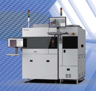
Chroma 7945 wafer chip inspection system is an automated inspection system for Pre and Post diced patterned wafers. Change kits enable switching between various applications by allowing different carriers including metal frame or grip ring.
Double Side Inspection
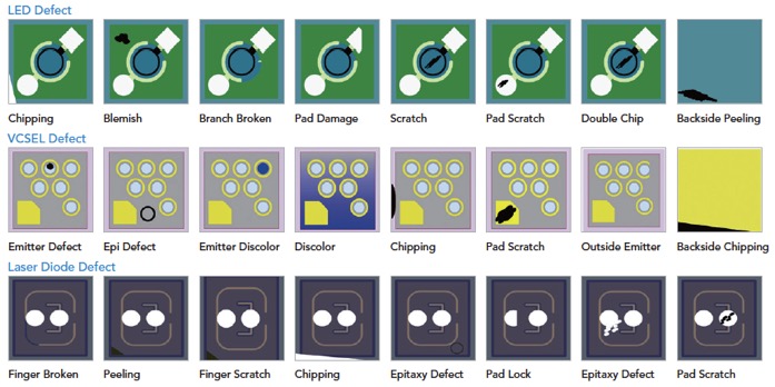
For compound semiconductor wafers, critical backside defects can occur during the dicing process (peeling, chipping, etc.) leading to catastrophic failure. To view such defects in traditional inspection systems the wafer (on tape) is flipped for backside inspection. This flipping with a second inspection run reduces a standard system's throughput by half, renders die loss (falling off of the inverted tape) and alignment challenges in front to backside wafer map correlation. The double-sided solution alleviates these issues as dual cameras capture the top and bottom sides simultaneously in one scan. This targeted solution yields loss-free and precise wafer map correlation in one single pass.
Color System
Discoloration can show angstrom level defects that are undetected on UV Line Scan or BW camera systems. Chroma's design identifies minimal discoloring to ensure there is not a higher overkill or underkill during the inspection process. The intuitive software assists the development of the inspection items in defined die zones according to the characteristics of color.
Wafer Map Format
Chroma 7945 supports traditional wafer map formats and is compatible with; .csv, SEMI XML, SNIF, STIF, and KLARF. Chroma's Mapping Software allows wafer map stacking of pre and post-dicing inspection (front + back sides) as well as test yield maps to validate the dicing process and consolidate the material inspection and test yield all on one map.
Home | Solutions | Support | Press Center | About Chroma | Contact
Copyright © Chroma ATE, Inc. All Rights Reserved.